section in PDF
manual in PDF


|
|
|
| |
| Get this section in PDF |
Get entire manual in PDF |
|
Chapter 24: IXIA 40/100 Gigabit Ethernet Load Modules
This chapter provides details about Ixia's K2 40-Gigabit and 100-Gigabit Ethernet test modules—the specifications and features.
Ixia's K2 40-Gigabit and 100-Gigabit Ethernet test modules are the world's first IP network traffic generation and layer 2-7 measurement and analysis test solution. K2 load modules are engineered to meet the needs of product teams developing 40 Gb/s and 100 Gb/s network devices such as routers, switches, and communications devices. K2 modules can measure and analyze the performance of Higher Speed Ethernet (HSE) standard-compliant devices at line rate, and are compatible with Ixia's chassis and broad range of 10 Mbps, 100 Mbps, 1 Gbps, and 10 Gbps interfaces, allowing real-world, full product testing in a single box.
Ixia's 40 Gb/s and 100 Gb/s load modules provide network device developers the ability to test 40 GE and 100 GE hardware electronics at full line-rate operation. Early adopters of the HSE technology can use the Ixia test system to validate their compliance with the new PCS lane operation of the IEEE P802.3ba draft standard.
Ixia's K2 load modules are valuable to developers who are integrating firmware and software into new electronics hardware, or integrating optical transceivers into their network devices and systems. Ixia's HSE modules can be used to validate and benchmark the performance limits of these network devices by employing layer 2 and 3 stress testing, virtual scalability testing, and negative testing. Ixia's HSE load modules ensure that a network device is ready to interoperate with other manufacturers' devices that claim compliance to the IEEE P802.3ba draft standard, and facilitate interoperability testing between different vendors of network devices and equipment.
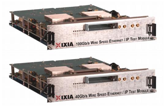
Figure 24-1. 100GE and 40GE LSM XMV Load Modules
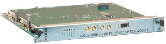
Figure 24-2. 40GE LSM XMV QSFP Load Module
Key Features
Industry's first 40 Gb/s and 100 Gb/s Layer 2 through 7 IP test solutions:
Industry's first commercially available 100 Gb/s Physical Coding Sublayer (PCS) test system:
Provides the ability to check compliance to the IEEE P802.3ba draft standard for both Transmit and Receive sides
Generates and analyzes full 40 Gb/s and 100 Gb/s line rate traffic:
Ixia's 40 Gb/s and 100 Gb/s load modules are designed for comprehensive layer 2-7 testing with integrated data plane and control plane traffic generation and analysis.
Nomenclature
The LSM HSE family identifying numbers are shown in Table 24-1.
Specification are given in Table 24-2..
HSE100GETSP1
HSE40/100GETSP1
100 Gbps
40GBASE-R
min-max
min-max
- User selected PRBS pattern for each PCS Lane
- User selects from a wide range of PRBS data patterns to be transmitted (true and complement)
- Send single, continuous, and exponentially controlled amounts of error injection
- Wide range of statistics, including: Pattern Lock, Pattern Transmitted, Pattern Received, Total Number of Bits Sent and Received, Total Number of Errors Sent and Received, Bit Error Ratio (BER), Number of Mismatched 1's and 0's.
- Lane Stats Grouping per lambda for SMF and MMF 40 Gb/s and 100 Gb/s based on IEEE802.3ba defined physical medium dependent (PMD).
Port LEDs
Each 40/100GE port incorporates a set of LEDs, as described in the following tables.
Clock In/Out
The load module provides coaxial connectors for clock input and clock output to allow the DUT to frequency-lock with the interface. When running off an external clock, the clock input signal must meet the requirements listed in Table 24-4 to ensure proper performance of the load module.
The clock in/out electrical interface parameters are also defined in Table 24-4.
The load module contains a phase-locked loop (PLL) that reduces the jitter of the input clock, either from the internal or external clock source. The bandwidth of the PLL is approximately 1kHz.
Statistics
Statistics for 40/100GE LSM cards, under various modes of operation may be found in Table B-36 on page B-165.
Intrinsic Latency Adjustment
This option, when present and enabled, reduces the measured latency by the amount of latency that is induced by the test equipment itself (not the DUT). For a specific transceiver, the system retrieves its pre-determined latency value and subtracts this from the measured overall latency. For an `unknown' transceiver (not previously measured), it calculates and stores the intrinsic latency value.
On the General tab in Port Properties, the Latency Calibration option is only enabled for cards with transceivers that have not been pre-measured for intrinisic latency by Ixia. The Latency Calibration option is grayed-out if any one of the following conditions are present:
The Latency Calibration option is enabled if the transceiver is CFP but no pre-calibrated value is found in the stored list. The Latency Calibration option is also enabled for transceivers that you have previously calibrated, so that the calibration measurement may be repeated (if desired).
Clicking the Latency Calibration option runs a Tcl script that measures intrinsic latency and stores the value in an .xml file. The .xml file contains the values that you have produced and saved. Each value is identified for a specific transceiver (per manufacturer, model, and serial number). You can run the calibrate process repeatedly with the same transceiver (if desired). Each new measurement overwrites the previous one for that transceiver.
Running the calibration measurement puts the port into a special loopback mode to measure intrinsic latency. When done, the port is put back into default normal mode. Any port configuration you have set before calibrating intrinsic latency, is lost as the port reverts to a default configuration.
The Enable check box is grayed out when no value exists in the system for the specific transceiver. If a value exists in the .xml file, then the Enable check box is available. Select the check box to enable the intrinsic latency adjustment.
After the intrinsic latency adjustment has been done, you may want to refresh the chassis or close and reopen the Port Properties dialog.
Multilane Distribution Configuration
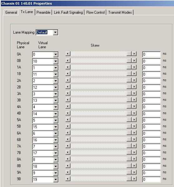
The Tx Lane tab allows to control the PCS (Physical Coding Sublayer) lane configuration and skew. It is part of the Port Properties for the module.
To open the Tx Lane tab:
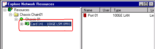
- Select the 40 or 100GE LSM XMV1 module in the left pane of the IxExplorer window as shown in Figure 24-3.
Figure 24-3. Select Module
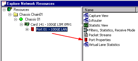
- Expand the node, and select the Port object. In the right window pane, double-click the Port Properties object as shown in Figure 24-4.
Figure 24-4. Port and Port Properties
- In the Port Properties dialog, select the Tx Lane tab. Use this tab to control the PCS lane order and the skew for each lane.
The Tx Lane tab is shown in Figure 24-5.
Figure 24-5. Tx Lane Tab
Table 24-5 explains the options in the Tx Lane tab page.
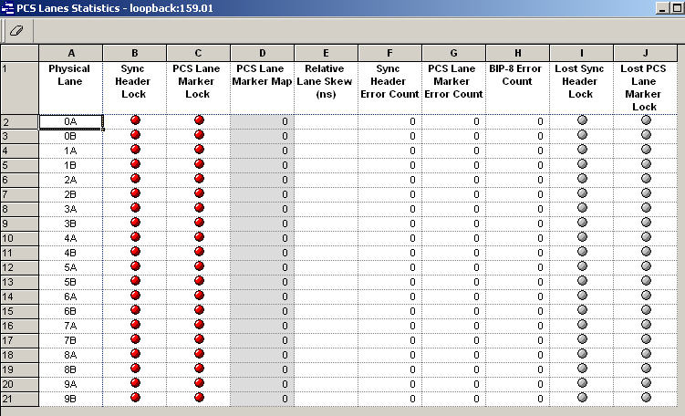
PCS Lane Statistics
The PCS lane statistics table allows to view the statistics for the configured PCS lanes.
To open the PCS lane statistics table:
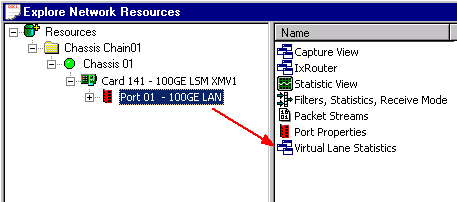
- Select the 40 or 100GE LSM XMV1 module in the left pane of the IxExplorer window as shown in Figure 24-3.
- Expand the node, and select the Port object. In the right window pane, double-click the PCS lane statistics object as shown in Figure 24-6.
Figure 24-6. Port and PCS Lane Statistics
- The PCS lane statistics table opens. Use this table to view the PCS lane statistics for each lane. The statistics are for the receive side.
The PCS lane statistics table is shown in Figure 24-7.
Figure 24-7. PCS Lane Statistics
TableTable 24-6 explains the entries in the PCS lane statistics table.
|
|
Did this document answer your question?
If not, let us know! |
|